


Meeting the Challenges in the Photovoltaic Cell Manufacturing Business
Share


 The challenges facing the photovoltaic industry of improving solar cell efficiency and reducing manufacturing costs while making the product appealing and economical in today’s highly competitive energy market have not changed. These are especially problematic when fossil fuels-based energy is once again having a resurgence.
Figure 1: Heterojunction type solar panel
Government subsidies enabled a huge expansion of the photovoltaic industry, but with their removal, the current market conditions become even more challenging for manufacturers. However, the photovoltaic cell manufacturing industry has been resilient, and after some reorganization and consolidation, it is now showing signs of an upturn. While the challenge is still to reduce costs, new technologies are being integrated into full scale manufacturing, which is not only challenging the status quo on industry costs, but is more importantly, increasing the efficiency of the photovoltaics. This is all very good for an industry as a whole and perhaps indicates the industry is starting to mature.
Historically, the photovoltaic market was dominated by thin film and the Crystalline (c-Si) photovoltaic cell manufacturing processes. In the last few years, the c-Si market has gained most of the market share, mostly due to cost. This has been to the detriment and almost led to the total demise of the thin film amorphous silicon (a-SI) market. Thin film Cadmium Telluride (CdTe) process has been an exception, and has been as successful as c-Si, again due to its low cost and high efficiency.
The resurgence in the photovoltaic market has seen the c-Si and the thin film processes join in a new alliance. Research shows the new technology potentially produces a cell of greater efficiency than the traditional c-Si cell with comparable costs. The technology doesn’t use CdTe thin film layers, but rather amorphous silicon thin film layers that are introduced into the more conventional crystalline silicon photovoltaic cell manufacturing process in order to generate higher efficiency solar panels.
Process change and risk review
This alliance of c-Si and a-Si processes brings together unique environmental challenges from both sides. The manufacture of high efficiency heterojunction-type photovoltaic panels introduces an amorphous silicon layer. The chambers are cleaned using fluorine gas that is often generated by using a plasma to break down a more benign gas, such as nitrogen trifluoride. Managing the waste byproducts, which include flammable, corrosive or condensable gases, the silica powder or waste water, is essential. Simple flow sheets for the treatment of waste gases from both crystalline and amorphous silicon layer manufacture are presented in figures 2 and 3.
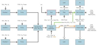

Figure 2: Process flow diagram for the management of
gases from the manufacture of crystalline silicon based
PV panels
Figure 3: Process flow diagram for the management of gases
from the manufacture of crystalline silicon and amorphous
silicon based PV panels in which chamber clean uses NF3.
(Lines as before, with red lines added where the risk profile
has changed because of the change of process.)
The process change needs chamber clean stages within the manufacturing cycle. Fluorine-based gases, such as nitrogen trifluoride, NF3, are activated either by remote or in-situ plasmas to generate fluorine for the purposes of performing the clean activity. The use of this clean step generates waste gases that contain untransformed clean gases (NF3), active clean gases (F2), and products of the reaction of the clean gas with the contamination on the chamber components (silicon tetrafluoride, SiF4). These waste gases represent a new challenge for the conventional crystalline photovoltaic industry in respect of their safe management from the tool, to the point-of-use gas treatment units, and then the management of the wastes generated by such processes.
The change of manufacturing process from conventional crystalline to a heterojunction, involving a fluorine-based chamber clean step, which is associated with the amorphous silicon deposition stage, requires careful forethought regarding the challenges presented by such a change.
Stewart Davidson is the brand and communications marketing manager at Edwards Vacuum.
Edwards Vacuum | www.edwardsvacuum.com
Volume: July/August 2015
.jpg?r=1919)
.jpg?r=1714)

.gif?r=7309)